
如何使STM32F446以180 Mhz运行?
我正试图让STM32F446全速运行,遵循本教程:https://www.youtube.com/watch?v=GJ_LFAlOlSk&t=826s我做了所有他做的事情,但是我的计时器的时钟速度非常慢,就像字面上说,当用标量为9和ARR为20的LED闪烁时,它很容易被眼睛看到。我做错了吗?
void setup_clock(void)
{
    // Enables HSE and waits until it is ready
    *RCC_CR |= (1 << RCC_CR_HSEON);
    while (!(*RCC_CR & (1 << RCC_CR_HSERDY)));

    // Set the power enable clock and voltage regulator
    *RCC_APB1ENR |= (1 << RCC_APB1ENR_PWREN);
    *PWR_CR |= PWR_CR_VOS(PWR_CR_VOS_SCALEM1);

    // Configure flash
    *FLASH_ACR = (1 << FLASH_ACR_DCEN) | (1 << FLASH_ACR_ICEN) | (1 << FLASH_ACR_PRFTEN);
    *FLASH_ACR |= FLASH_ACR_LATENCY(5);

    // Configures HCLK, PCLK1, PCLK2
    *RCC_CFGR &= ~RCC_CFGR_HPRE_MASK;
    *RCC_CFGR |= RCC_CFGR_HPRE(RCC_CFGR_HPRE_NODIV);    // HCLK 180Mhz

    *RCC_CFGR &= ~RCC_CFGR_PPRE1_MASK;
    *RCC_CFGR |= RCC_CFGR_PPRE1(RCC_CFGR_PPRE1_DIV4);   // PCLK1 45Mhz

    *RCC_CFGR &= ~RCC_CFGR_PPRE2_MASK;
    *RCC_CFGR |= RCC_CFGR_PPRE2(RCC_CFGR_PPRE2_DIV2);   // PCLK2 90Mhz

    // Configures the main PLL
    *RCC_PLLCFGR = RCC_PLLCFGR_PLLN(180) |
            RCC_PLLCFGR_PLLP(RCC_PLLCFGR_PLLP_2) |
            RCC_PLLCFGR_PLLR(2) |
            RCC_PLLCFGR_PLLM(4) |
            (1 << RCC_PLLCFGR_PLLSRC);

    // Enable PLL
    *RCC_CR |= (1 << RCC_CR_PLLON);
    while (!(*RCC_CR & (1 << RCC_CR_PLLRDY)));

    // Use PLL as clock source
    *RCC_CFGR &= ~RCC_CFGR_SW_MASK;
    *RCC_CFGR |= RCC_CFGR_SW(RCC_CFGR_SW_PLL_P);
    while ((*RCC_CFGR & RCC_CFGR_SWS_MASK) != RCC_CFGR_SWS(RCC_CFGR_SWS_PLL));

    // Sets the CLOCK Ready status LED
    *GPIO_ODR(STATUS_BASE) |= (1 << STATUS_CLKREADY);
}回答 2
Stack Overflow用户
发布于 2020-12-04 18:56:36
下面是使用gnu的NUCLEO_F44RE的一个完整的工作项目,您需要构建和运行所有这些工具。
差异。
我是从默认的电源模式开始的(看起来是这样的,是吗?),所以保守地将闪存除数设置为8(9个时钟)。(可以尝试之后,我会亲自设置8,首先让它工作,然后工作回到5)。
我既不使用I也不使用D缓存。
我将系统设置为HSE,然后设置PLL来使用它。跳过这一步,这可能很好,因为HSE已经启动并准备好了(供PLL使用)。
这条线
*RCC_CFGR &= ~RCC_CFGR_SW_MASK;将时钟切换到HSI,然后
*RCC_CFGR |= RCC_CFGR_SW(RCC_CFGR_SW_PLL_P);把时钟切换到锁相环。需要下定决心,不要像Lundin评论的那样使用/滥用寄存器。您应该做干净的读-修改-写,读,零的位需要零(或所有在字段中)设置的位,然后写到寄存器。为此使用临时变量。或者是某种味道
reg = (reg&this) | that;但肯定不是
reg &= this;
reg |= that;
总体而言。我怀疑这不是你的问题,though...Just是我们几个/几个人的评论。
您的PLLQ处于无效状态。可能有问题,试试看。
我正在为皮层构建-M0出于习惯/可移植性的代码,可以很容易地改变。
在PJ提出来之前
*RCC_APB1ENR |= (1 << RCC_APB1ENR_PWREN);
*PWR_CR |= PWR_CR_VOS(PWR_CR_VOS_SCALEM1);
您需要检查编译后的输出是有风险的,它可能会根据编译器、版本、月亮的相位而变化。如果str到RCC_APB1ENR的后面紧跟PWR_CR的LDR,则可能不起作用。我所看到的基于PJ对另一张票的评论所做的实验是,gpio (在那里是这样的),由于某种原因,您可以通过关闭外围设备读取MODER寄存器,从而使MODER的enable的str工作,那么修改和写入的指令就会超过写入的时间。但是如果您阻塞moder寄存器,并且具体取决于您的编译器和设置,它可以将它们优化为两个背靠背存储,我能够用一个编译器而不是另一个编译器来实现这一点。(更改设置,它们会修复和失败,等等)。我所做的GET32 32/PUT32 32确保在启用之前触摸外围设备没有问题。YMMV
flash.s
.cpu cortex-m0
.thumb

.thumb_func
.global _start
_start:
.word 0x20001000
.word reset

.thumb_func
reset:
    bl notmain
    b hang
.thumb_func
hang:   b .

.thumb_func
.globl PUT32
PUT32:
    str r1,[r0]
    bx lr

.thumb_func
.globl GET32
GET32:
    ldr r0,[r0]
    bx lr
flash.ld
MEMORY
{
    rom : ORIGIN = 0x08000000, LENGTH = 0x1000
}
SECTIONS
{
    .text   : { *(.text*)   } > rom
}
notmain.c
void PUT32 ( unsigned int, unsigned int );
unsigned int GET32 ( unsigned int );
void dummy ( unsigned int );

#define RCCBASE         0x40023800
#define RCC_AHB1ENR     (RCCBASE+0x30)

#define RCC_CR           (RCCBASE+0x00)
#define RCC_PLLCFGR         (RCCBASE+0x08)
#define RCC_CFGR         (RCCBASE+0x08)

#define FLASH_ACR       0x40023C00

#define GPIOABASE       0x40020000
#define GPIOA_MODER     (GPIOABASE+0x00)
#define GPIOA_BSRR      (GPIOABASE+0x18)

//PA5

#define STK_CSR 0xE000E010
#define STK_RVR 0xE000E014
#define STK_CVR 0xE000E018

static void clock_init ( void )
{
    unsigned int ra;

    //switch to external clock.
    ra=GET32(RCC_CR);
    ra|=1<<16;
    PUT32(RCC_CR,ra);
    while(1) if(GET32(RCC_CR)&(1<<17)) break;
    if(1)
    {
        ra=GET32(RCC_CFGR);
        ra&=~3;
        ra|=1;
        PUT32(RCC_CFGR,ra);
        while(1) if(((GET32(RCC_CFGR)>>2)&3)==1) break;
    }
    //HSE ready
}

static void pll_init ( void )
{
    unsigned int ra;

    //clock_init();

    ra=GET32(FLASH_ACR);
    ra&=(~(0xF<<0));
    ra|=(    8<<0);
    PUT32(FLASH_ACR,ra);
    //poll this?

    ra=GET32(RCC_CFGR);
    ra&=(~(0x3<<13));
    ra|=(    4<<13); //180/90 = 2
    ra&=(~(0x3<<10));
    ra|=(    5<<10); //180/45 = 4
    PUT32(RCC_CFGR,ra);

    //HSE 8Mhz
    //PLLM It is recommended to select a frequency of 2 MHz to limit
    //  PLL jitter.
    //PLLN input is 2, want >=50 and <=432 so between 25 and 216
    //PLLM 4, PLLN 180, VCO 360, PLLP 2
    //PLLM 8/4 = 2
    //PLLN 2 * 180 = 360
    //PLLP 360 / 2 = 180
    //PLLR 2?
    //PLLQ 180 / 48 = 3.75 so 4.
    ra=0;
    ra|=2<<28;  //PLLR
    ra|=4<<24;  //PLLQ dont care
    ra|=1<<22;  //PLLSRC HSE
    ra|=2<<16;  //PLLP
    ra|=180<<6; //PLLN
    ra|=4<<0;   //PLLM
    PUT32(RCC_PLLCFGR,ra);
    ra=GET32(RCC_CR);
    ra|=1<<24;
    PUT32(RCC_CR,ra);
    while(1) if(GET32(RCC_CR)&(1<<25)) break;
    ra=GET32(RCC_CFGR);
    ra&=~3;
    ra|=2;
    PUT32(RCC_CFGR,ra);
    while(1) if(((GET32(RCC_CFGR)>>2)&3)==2) break;
}

static void led_init ( void )
{
    unsigned int ra;

    ra=GET32(RCC_AHB1ENR);
    ra|=1<<0; //enable GPIOA
    PUT32(RCC_AHB1ENR,ra);

    ra=GET32(GPIOA_MODER);
    ra&=~(3<<(5<<1)); //PA5
    ra|= (1<<(5<<1)); //PA5
    PUT32(GPIOA_MODER,ra);
}

static void led_on ( void )
{
    PUT32(GPIOA_BSRR,((1<<5)<< 0));
}

static void led_off ( void )
{
    PUT32(GPIOA_BSRR,((1<<5)<<16));
}

void do_delay ( unsigned int sec )
{
    unsigned int ra,rb,rc,rd;

    rb=GET32(STK_CVR);
    for(rd=0;rd<sec;)
    {
        ra=GET32(STK_CVR);
        rc=(rb-ra)&0x00FFFFFF;
        if(rc>=16000000)
        {
            rb=ra;
            rd++;
        }
    }
}

int notmain ( void )
{
    unsigned int rx;

    led_init();

    PUT32(STK_CSR,0x00000004);
    PUT32(STK_RVR,0xFFFFFFFF);
    PUT32(STK_CSR,0x00000005);

    for(rx=0;rx<5;rx++)
    {
        led_on();
        while(1) if((GET32(STK_CVR)&0x200000)!=0) break;
        led_off();
        while(1) if((GET32(STK_CVR)&0x200000)==0) break;
    }
    clock_init();
    for(rx=0;rx<5;rx++)
    {
        led_on();
        while(1) if((GET32(STK_CVR)&0x200000)!=0) break;
        led_off();
        while(1) if((GET32(STK_CVR)&0x200000)==0) break;
    }
    pll_init();
    while(1)
    {
        led_on();
        while(1) if((GET32(STK_CVR)&0x200000)!=0) break;
        led_off();
        while(1) if((GET32(STK_CVR)&0x200000)==0) break;
    }


    return(0);
}
构建
arm-linux-gnueabi-as --warn --fatal-warnings -mcpu=cortex-m0 flash.s -o flash.o
arm-linux-gnueabi-gcc -Wall -O2 -ffreestanding -mcpu=cortex-m0 -mthumb -c notmain.c -o notmain.o
arm-linux-gnueabi-ld -nostdlib -nostartfiles -T flash.ld flash.o notmain.o -o notmain.elf
arm-linux-gnueabi-objdump -D notmain.elf > notmain.list
arm-linux-gnueabi-objcopy -O binary notmain.elf notmain.bin
(你可以自然地将大脑皮层-M0改为皮层-M4)。
将notmain.bin复制到核卡上,并观察用户引导的变化速度。更快,更慢,更快。
嗯..。
when VOS[1:0] = '0x11, the maximum value of f HCLK is 168 MHz. It can be extended to 180 MHz by activating the over-drive mode. The over-drive mode is not available when VDD ranges from 1.8 to 2.1 V (refer to Section 5.1.3: Voltage regulator for details on how to activate the over-drive mode).和
11: Scale 1 mode (reset value)(所以没必要搞砸了)
和
Entering Over-drive mode
It is recommended to enter Over-drive mode when the application is not running critical
tasks and when the system clock source is either HSI or HSE. To optimize the configuration
time, enable the Over-drive mode during the PLL lock phase.
To enter Over-drive mode, follow the sequence below:
Note:
1. Select HSI or HSE as system clock.
2. Configure RCC_PLLCFGR register and set PLLON bit of RCC_CR register.
3. Set ODEN bit of PWR_CR register to enable the Over-drive mode and wait for the
ODRDY flag to be set in the PWR_CSR register.
4. Set the ODSW bit in the PWR_CR register to switch the voltage regulator from Normal
mode to Over-drive mode. The System will be stalled during the switch but the PLL
clock system will be still running during locking phase.
5. Wait for the ODSWRDY flag in the PWR_CSR to be set.
6. Select the required Flash latency as well as AHB and APB prescalers.
7. Wait for PLL lock.
8. Switch the system clock to the PLL.
9. Enable the peripherals that are not generated by the System PLL (I2S clock, SAI1 and
SAI2 clocks, USB_48MHz clock....).
所以我是在室温下运行的,芯片离最高温度很近,所以很可能它的工作原理很好,就像我在这里所做的那样。(从技术上讲,它不是完全需要的,要么是168,要么设置为超速驱动)。
如果您想要180 vs 168,您应该按照文档执行这些步骤。
我怀疑你没有在最高温度附近运行你的部分,所以你也应该能够逃脱180。尝试删除您的pwr注册材料,看看这是否有帮助,使您的闪存延迟更长,等等。改为168 pwr,等等。
你是尝试180出大门,还是你尝试了一些更合理的速度,先不推任何边缘,比如小于45兆赫,然后在45到90之间,然后再工作到180?
编辑
The Flash memory interface accelerates code execution with a system of instruction prefetch and cache lines.

Main features
• Flash memory read operations
• Flash memory program/erase operations
• Read / write protections
• Prefetch on I-Code
• 64 cache lines of 128 bits on I-Code
• 8 cache lines of 128 bits on D-CodeStack Overflow用户
发布于 2020-12-04 19:01:45
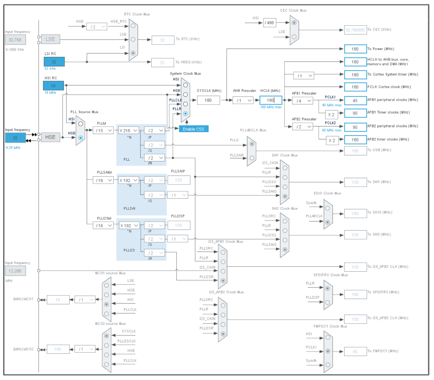
CubeMx有一个非常方便的时钟配置工具。我不使用HAL,但这个工具节省了很多时间。
正如我所看到的,您试图通过使用自己的寄存器定义来重新发明轮子。使用标准的CMSIS作为创建自己的CMSIS没有任何意义。
这是不可能有180 the时钟和使用USB在同一时间,因为你不能得到48兆赫要求的USB外设。
这里有一些可能的设置:25 osc外部osc:
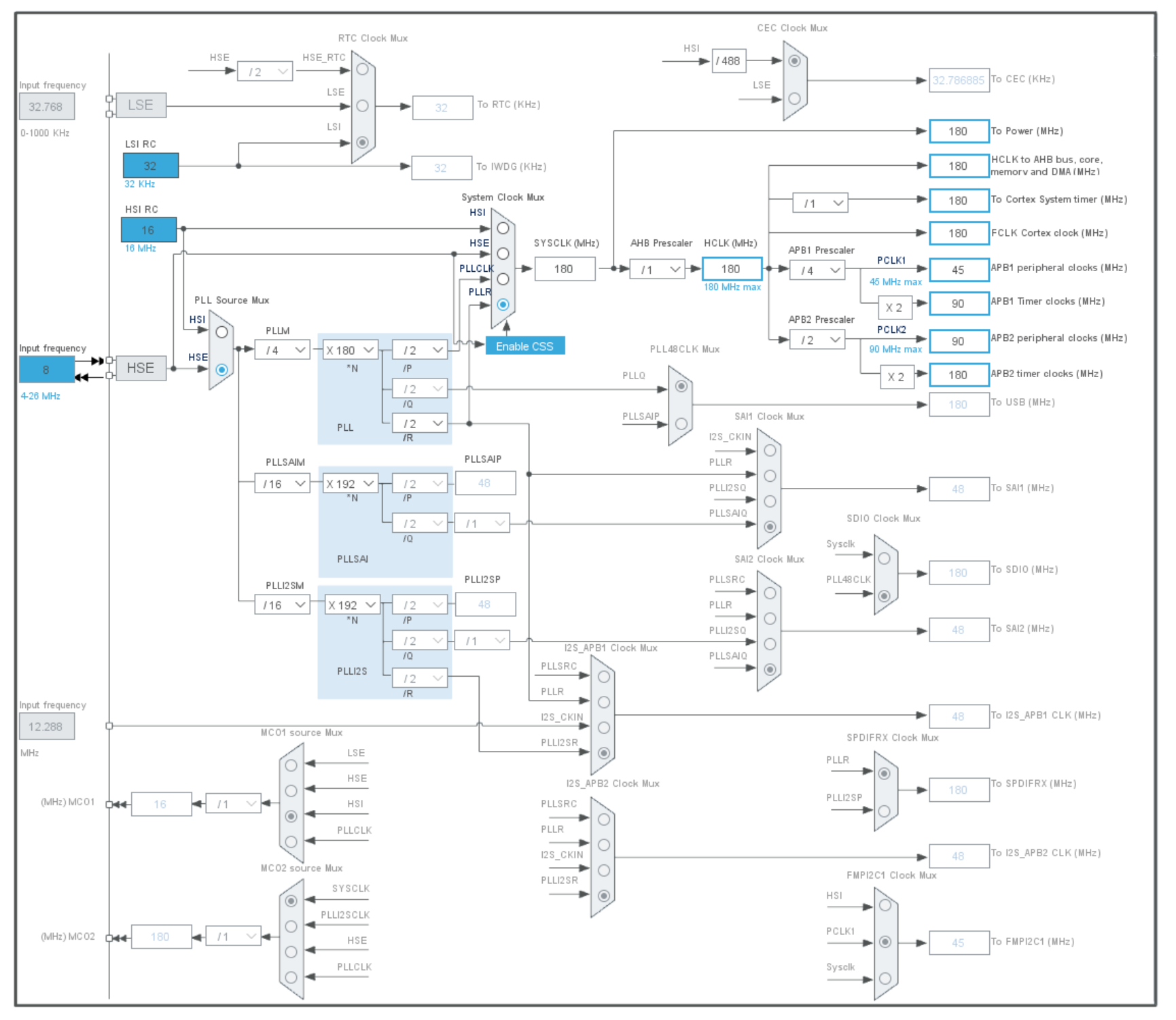
8 8Mhz外部osc:
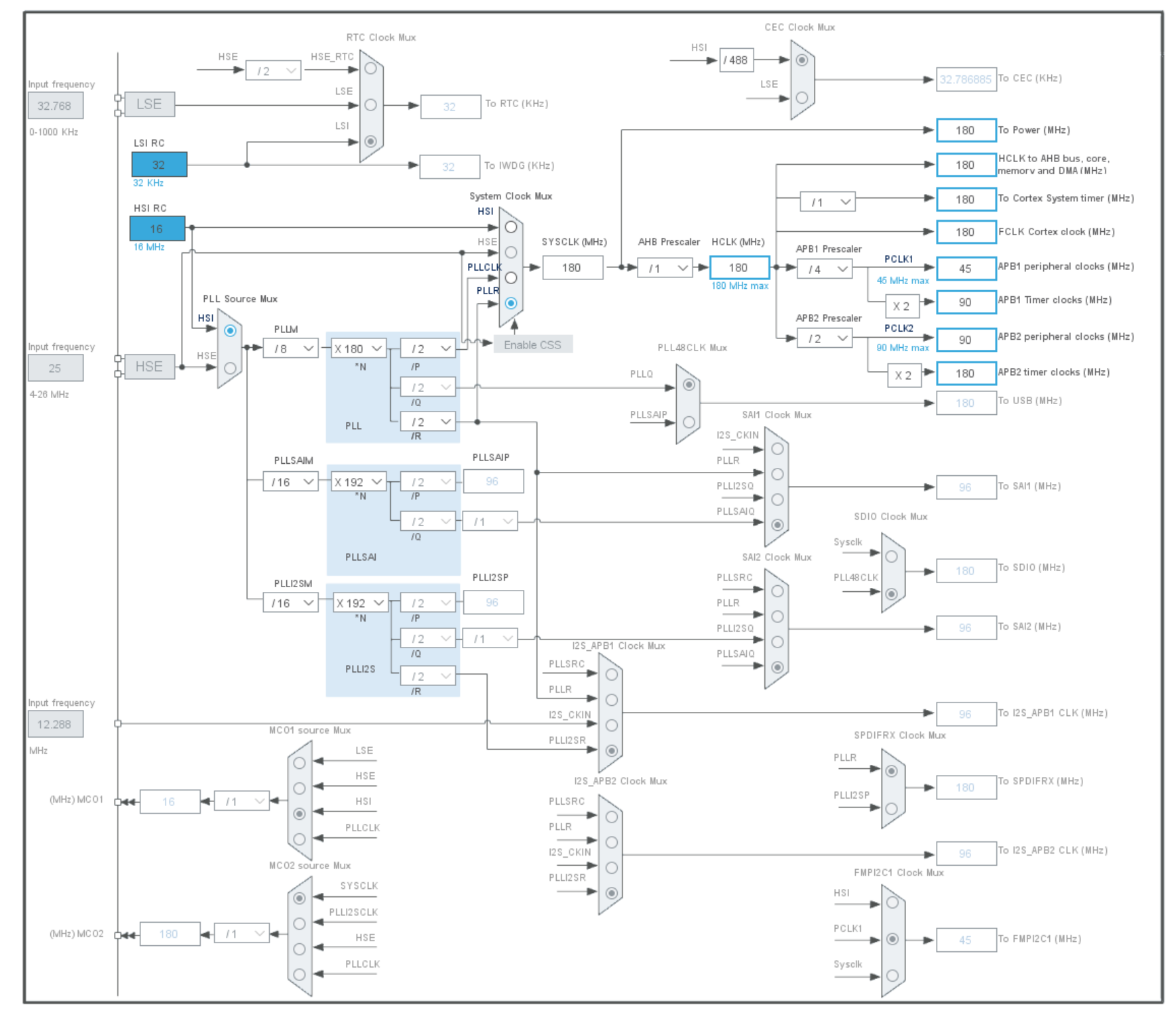
18 osc内部osc
https://stackoverflow.com/questions/65145553
复制相似问题
腾讯云开发者
