stm32f4将16位写入两个8位gpio端口
提问于 2018-01-21 00:52:40
我试图将16位数据写入两个选定的8位gpio端口.我必须拆分LSB和MSB的数据:
void LCD_write_command(uint16_t cmd) {
    GPIOD->ODR = cmd & 0x00ff; //lsb
    GPIOA->ODR = (GPIOA->ODR & 0x00ff) | (cmd >> 8); //msb
}
并阅读数据:
uint16_t LCD_read_data(void) {
    (here is instruct gpio as input)
    volatile uint16_t data = 0;
    data  = (uint16_t)GPIOD->IDR & 0x00ff; //lsb
    data |= (uint16_t)GPIOA->IDR << 8 ; // msb
    (here is instruct gpio as output)
    return data;
}
当我使用一个16位的gpio来写和读时,一切都很好:
 void LCD_write_command(uint16_t cmd) {
    GPIOD->ODR = cmd & 0xffff;
}
uint16_t LCD_read_data(void) {
    volatile uint16_t data = 0;
    data  = (uint16_t)GPIOD->IDR & 0xffff;
    return data;
}
我不知道我错过了什么。

回答 4
Stack Overflow用户
回答已采纳
发布于 2018-01-22 05:29:36
wtite_bits(uint16_t cmd)
{
    uint32_t data = GPIOA -> ODR;

    data &= ~(0x1fff);
    data |= cmd & 0x1fff;
    GPIOA -> ODR = data;

    data = GPIOB -> ODR;
    data &= ~(0x0007);
    data |= (cmd & 0x8fff) >> 13;
    GPIOB -> ODR = data;
}
保存寄存器中的其他位
Stack Overflow用户
发布于 2018-01-21 02:07:44
您需要学习更多关于按位操作的知识。
- 写作 LCD_write_command(uint16_t cmd) { uint32_t tmp = GPIOD->ODR;tmp &= ~(0xff);tmp |= (cmd & 0x00ff);uint32_t->ODR= tmp;//uint32_t tmp = GPIOA->ODR;tmp &= ~(0xff);tmp |= (cmd >> 8);GPIOA->ODR;//msb }
或
void LCD_write_command(uint16_t cmd) {
   *(volatile uint8_t *)&GPIOD->ODR = cmd & 0xff;
   *(volatile uint8_t *)&GPIOA->ODR = cmd >> 8; //msb
}
强制编译器使用8位存储指令。
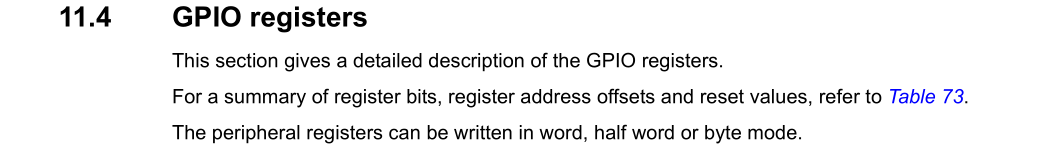
在使用非字访问寄存器之前,检查RM中是否允许:
Stack Overflow用户
发布于 2018-01-21 07:50:13
非你的建议代码为我工作,以下是原来的源代码处理LCD:
void LCD_write_command(uint16_t cmd) {
    GPIOB->BRR = LCD_CS;       // LCD_CS low (chip select pull)
    GPIOB->BRR = LCD_RS;       // LCD_RS low (register select = instruction)
    //GPIOA->ODR = cmd;         // put cmd to PortA (full length)
    // put cmd [0..12] bits to PortA (actual LCD_DB00..LCD_DB12)
    // put cmd [13..15] bits to PortB (actual LCD_DB13..LCD_DB15)
    GPIOA->ODR = cmd & 0x1fff;
    GPIOB->ODR = (GPIOB->ODR & 0xfff8) | (cmd >> 13);
    GPIOB->BRR = LCD_WR;       // pull LCD_WR to low (write strobe start)
    // Write strobe 66ns long by datasheet. GPIO speed on STM32F103 at 72MHz slower -> delay is unnecessary
    // asm volatile ("nop");
    GPIOB->BSRR = LCD_WR;      // pull LCD_WR to high (write strobe end)
    GPIOB->BSRR = LCD_CS;      // LCD_CS high (chip select release)
}
我检查了RM,我可以做8位,半字一字的手术。
页面原文内容由Stack Overflow提供。腾讯云小微IT领域专用引擎提供翻译支持
原文链接:
https://stackoverflow.com/questions/48365156
复制


腾讯云开发者
